 by
by Introduction
Chemical mechanical planarization (CMP) slurry plays a crucial yet often overlooked role in the semiconductor manufacturing process. As chip designs grow ever smaller and more complex, CMP slurry has become an essential part of the microlithography techniques needed to produce integrated circuits. This article discusses the purpose of CMP slurry, how it works, different types of slurry, and new developments that will push the boundaries of semiconductor technology.
What is CMP slurry?
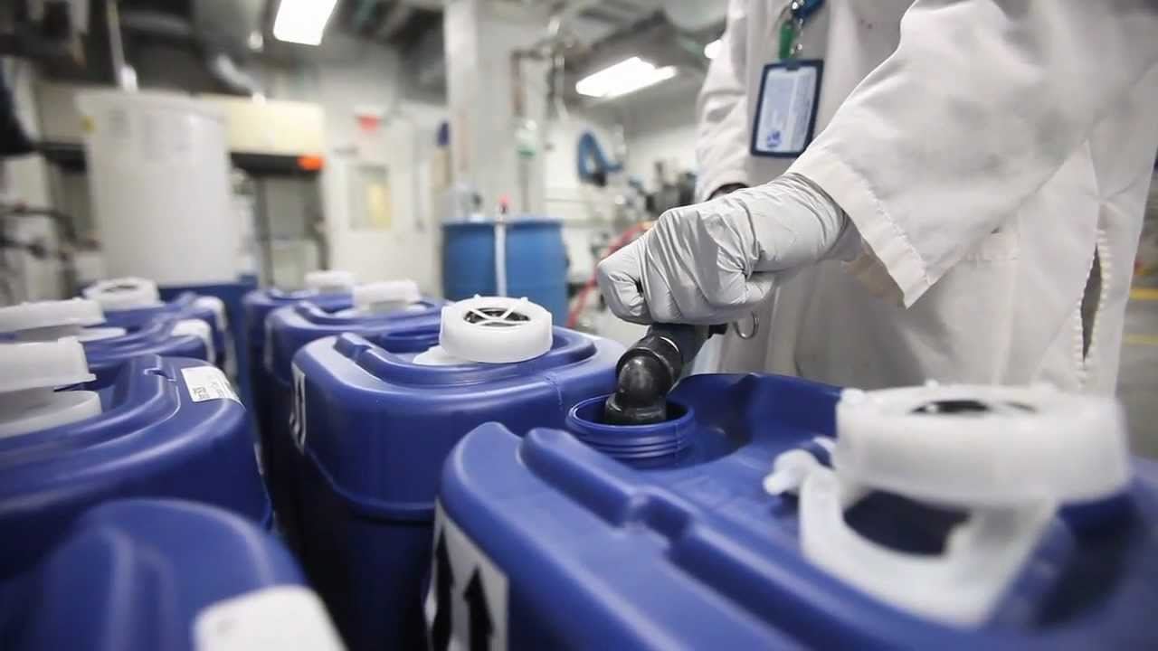
A CMP slurry is a liquid solution that is used during the chemical mechanical planarization or chemical mechanical polishing (CMP) process. CMP is used to planarize or flatten the surface of a wafer during the production of semiconductors and integrated circuits. It involves using both chemical and mechanical forces to polish away excess material on the wafer and leave a very flat surface. At the core of CMP is the slurry, which contains nano-sized abrasive particles such as silica or ceria suspended in an alkaline or acidic solution.
During CMP, the wafer is placed facedown on a polishing pad and slight pressure is applied. Slurry is dispersed across the pad and the wafer is rotated back and forth. The abrasive particles in the slurry help grind down surfaces as the chemicals in the solution interact and dissolve materials. This dual chemical and mechanical action allows a very precise, highly polished finish on the wafer surface needed for ever smaller circuit designs. Without a high-quality slurry, it would be impossible to attain the smooth, mirror-like wafer surfaces required by modern chip manufacturers.
Types of CMP slurries
Several different types of slurries are commonly used depending on the material being polished. For polishing oxide materials such as silicon dioxide, slurries containing silica or ceria particles suspended in an alkaline solution are generally employed. These abrasives combined with the chemical activity of the base help efficiently remove oxide layers.
For polishing metal films such as tungsten, copper, or aluminum, slurries containing various metal oxides in acidic solutions are preferred. The acidity aids in dissolving the polishing target material while the abrasives grind it away. Multipurpose slurries have also been developed that can planarize both dielectrics and metals in a single step.
Specialty slurries are additionally being formulated for polishing harder and more challenging materials like low-k dielectrics, which are important insulators with lower dielectric constants that help minimize signal delays in transistors. Maintaining consistent and optimized slurry chemistry is crucial for achieving uniform polishing across entire wafer surfaces.
Advancing slurry technology
As the semiconductor industry progresses towards ever smaller nodes below 10 nanometers, new demands are being placed on CMP slurry performance and composition. Chipmakers require slurries that can remove material with greater selectivity, leave virtually no defects or residue, and withstand higher pressures and down forces. This is driving the need for continued advances in slurry R&D.
Some new slurry formulations aim to increase selective polishing rates between dielectrics vs metals or between different metals. By tuning particle size, zeta potential, and chemical additives, slurries can be designed for preferential removal of one material over another. Other developments focus on using new complexing and synergistic chemistries to enhance material dissolution while minimizing defects.
Nanoparticle engineering is another active area of slurry innovation. Manipulating particle size, shape, composition and surface functionalization allows achieving better polishing efficiency and controls over critical parameters like wafer uniformity. Some companies are exploring novel ceramic particles and core-shell particles with tunable properties. Real-time particle monitoring during CMP is also being commercialized to ensure consistent slurry performance.
Additionally, as 3D stacking and heterogeneous integration become more widespread, novel slurry types must be qualified for applications like through-silicon via formation. With the industry roadmap pushing beyond the 3nm node within the next decade, further leaps in slurry technology will be paramount to overcoming the manufacturing challenges ahead. Sustained R&D investment ensures CMP slurry continues to enable Moore’s Law and advancement of the global semiconductor ecosystem.
Conclusions
Invisible to consumers but essential for all modern electronics, CMP slurry is the unsung hero that helps drive the miniaturization behind today’s advanced microchips. Just as IC designs evolve in complexity, slurry technology must also advance to support the polishing needs of wafer fabs producing at smaller technology nodes. With the semiconductor industry forecast to become a $1 trillion by 2030, refining this critical material promises to remain a priority focus area for equipment suppliers and slurry formulators alike. Continued progress in slurry chemistry and engineering will be required to realize the smallest of future nanoelectronic devices still on the horizon.
*Note:
- Source: Coherent Market Insights, Public sources, Desk research
- We have leveraged AI tools to mine information and compile it