 by
by Wet chemicals play a crucial role in the manufacturing and processing of semiconductors and electronics. From silicon wafers to printed circuit boards, wet chemicals are indispensable for cleaning, etching, growing films and other processing steps. In this article, we will explore the various types of wet chemicals used in electronics and semiconductor applications along with their functions.
Cleaning Wet Chemicals
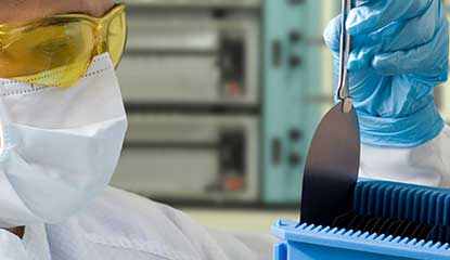
One of the most fundamental uses of wet chemicals is for cleaning semiconductor wafers and electronic components. Dirty surfaces need to be thoroughly cleaned before subsequent processing steps such as lithography, deposition, etching etc. Various types of cleaning solutions are used including:
– Acidic cleaners – Acids like hydrofluoric acid (HF), hydrochloric acid (HCL), nitric acid (HNO3) etc. are used to dissolve and remove metallic contaminants and native oxide layers from surfaces.
– Alkaline cleaners – Caustic solutions like ammonium hydroxide (NH4OH) and sodium hydroxide (NaOH) remove organic contamination through saponification. They also dissolve native oxides formed during acidic cleaning.
– Solvents – Organic solvents like acetone, isopropanol (IPA) help dissolve and flush away particulate contamination. Solvents are also used for drying wafers after wet cleaning steps.
– Deionized water (DI water) – High purity DI water is used extensively after each wet cleaning step to rinse away dissolved contaminants and residues of prior cleaning solutions.
Thorough cleaning of surfaces with precise mixes of wet chemicals is critical to obtain defect-free surfaces for high-yield manufacturing of electronics.
Etch Wet Chemicals
Etching is another key processing step where specific patterns or layers are removed by selectively exposing surfaces to chemical etchants. Commonly used etch chemistries include:
– Hydrofluoric acid (HF) – A very common etchant used for silicon dioxide (SiO2), silicon nitride (Si3N4) and semiconductors. Dilute HF dissolves native oxides for cleaning.
– Buffered oxide etch (BOE) – Mixture of HF and ammonium fluoride (NH4F) provides smooth, uniform etching of SiO2 and is widely utilized for shallow trench isolation and contact hole etching in CMOS fabrication.
– Potassium hydroxide (KOH), Tetramethylammonium hydroxide (TMAH) – Used for anisotropic chemical etching of single crystal silicon in MEMS and semiconductor device manufacturing.
– Hydrochloric acid (HCl) – Etches metals like aluminum, tungsten and alloys. Hot HCl solution removes TiN barrier layers.
– Nitric acid (HNO3) – Dissolves silicon very slowly but effectively removes organic residues making it suitable for cleaning prior to certain deposition steps.
Wet chemical etchants enable precise control over patterns and profiles during device structuring which is critical for functionality and performance.
Thin Film Deposition Wet Chemicals
A plethora of thin film deposition techniques in semiconductor manufacturing rely on wet chemical solutions:
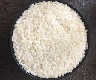
– Chemical vapor deposition (CVD) precursors – Liquid sources of gases like silane (SiH4), disilane (Si2H6), germane (GeH4) are transported into CVD reactors using bubblers containing wet chemicals.
– Metalorganics – Alkyl derivatives of metals such as tetramethylsilane (TMS), trimethylaluminum (TMA) used in MOCVD are handled as wet precursors.
– Atomic layer deposition (ALD) precursors – Similarly, ALD relies on sequential pulsing of metalorganic precursors which are supplied from liquid sources.
– Electroplating solutions – Solutions of metal salts like copper sulfate, gold cyanide, nickel chloride for plating of on-chip interconnects in damascene processes.
– Solution growth – Compounds like CdTe, GaAs are grown in tanks of thiourea, cadmium chloride and organometallic solutions through low cost techniques.
Wet chemical precursors enable deposition of a wide variety of thin films with atomic scale precision which serve as the building blocks of semiconductor components.
Post Etch and Deposition Wet Processes
Cleaning away residues of previous steps is critical for yield and device performance:
– Post etch residues – Rinsing with mixtures of acids and solvents removes polymer debris from deep feature etches.
– Post deposition residues – ALD or CVD films may require solvent cleaning using acetone or special additives in SC1 alkaline mixtures.
– Post plating cleaning – Electroplated layers need cleaning in chemical solutions to remove salts and contamination introduced during the plating process.
– Ion implantation contamination – Wafers implanted with dopants require cleaning to remove intermixing products at the surface before gate oxidation or metallization.
Careful wet cleaning after critical steps prevents harm to underlying layers and reduces defects from foreign matter introduced earlier in the flow.
Reliability and Packaging Wet Chemicals for Electronics and Semiconductor
As semiconductor technologies shrink and complexity increases, focus on reliability grows:
– Corrosion inhibitors – Compounds like benzotriazole (BTA) are used to passivate metal surfaces and prevent electrochemical corrosion.
– Anti-reflective coatings (ARC) – Wet chemicals deposit thin ARC films to reduce scattering effects during lithography of advanced nodes.
– Wet surface treatments – Solutions passivate defects at interfaces to improve device lifetimes through effects like negative bias temperature instability (NBTI).
– Encapsulants – Potting and sealing compounds protect integrated circuits and chips from moisture and mechanical stresses during manufacturing tests and in finished products.
Reliable performance over product lifetimes relies heavily on judicious use of wet chemical treatments at each manufacturing stage and in packaging.