by
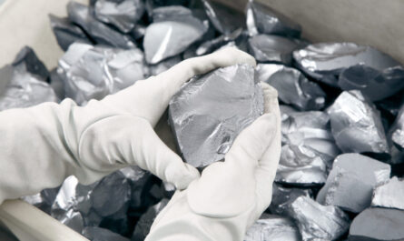
by Physical vapor deposition is a vacuum process used to produce thin films through the condensation of a vaporized form of the desired material onto various surfaces. Physical vapor deposition is widely used in a variety of applications such as electronics, optics, medical devices, tribological components, and hard materials. The global physical vapor deposition market is estimated to be valued at US$ 18.09 Bn in 2023 and is expected to exhibit a CAGR of 5.5% over the forecast period 2023 to 2030, as highlighted in a new report published by Coherent Market Insights.
The semiconductor industry has been witnessing rapid growth attributed to the boom in consumer electronics and proliferation of IoT devices. Physical vapor deposition plays a crucial role in manufacturing semiconductors and integrated circuits as it is used to deposit thin films of materials like tungsten, aluminum, and titanium nitride. Rising demand for advanced semiconductor devices is propelling the adoption of physical vapor deposition among semiconductor manufacturers.
Market key trends:
The increasing adoption of physical vapor deposition in the semiconductor industry remains one of the major factors driving the market growth. Over the recent past, there has been significant increase in spending on semiconductor fabrication equipment attributed to high investments by foundry companies to boost manufacturing capacity. According to Semiconductor Equipment and Materials International (SEMI), global sales of semiconductor manufacturing equipment are expected to grow over 15% year-over-year in 2021, indicating rising spend of foundries on fabrication equipment including physical vapor deposition systems. Continuous technological advancements to develop more efficient and advanced physical vapor deposition systems are further expected to support the market expansion over the forecast period.
SWOT Analysis
Strength: Physical Vapor Deposition (PVD) technology has applications in various industries like consumer electronics, automotive, medical devices and more. It provides thin film coatings with excellent uniformity and adhesion.
Weakness: PVD processes are more complex and expensive compared to alternative coating technologies. Initial capital investments are high for setting up PVD equipment.
Opportunity: Growing demand for microelectronics components and solar panels will drive opportunities for PVD in semiconductor fabrication and photovoltaic industries. Emerging applications of PVD coatings in the medical devices sector also present growth prospects.
Threats: Advancements in alternative coating technologies like Chemical Vapor Deposition (CVD) pose a threat by replacing some PVD applications over time. Trade barriers and geopolitical issues can disrupt supply chains for PVD equipment and components.
Key Takeaways
The global Physical Vapor Deposition market is expected to witness high growth over the forecast period of 2023 to 2030 on account of expanding applications across various end-use sectors. The market size is projected to reach US$ 18.09 Billion by 2024.
Regional analysis: Asia Pacific accounts for the largest share of the global PVD market currently due to presence of consumer electronics manufacturing bases in countries like China, South Korea and Taiwan. China has emerged as the dominant player accounting for more than 30% market share in Asia Pacific attributed to large semiconductor fabrication activities. Fast growing countries in Southeast Asia too are expected to drive regional growth.
Key players: Key players operating in the Physical Vapor Deposition market are Oerlikon Balzers (Oerlikon Group), IHI Corporation, Silfex Inc., Lam Research Corp, Singulus Technologies AG, Applied Materials, Inc., ULVAC Inc., Veeco Instruments Inc., Buhler AG, Semicore Equipment, Inc., and Platit AG. The market remains quite consolidated with top players dominating the equipment supply landscape.